RF Bandpass Filter
Tackling the Bandpass Filter Design
Fresh off the success of project 1, I dove into the second project for my microwaves class, a bandpass filter design that tested my RF skills in a new way. This project had me designing a filter for a microwave device company, working with stripline transmission on Rogers RT/Duroid 5880 substrate. With my ADS workspace ready and results in hand, here’s a rundown of my journey!
The Mission
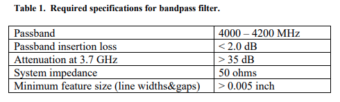
The goal was to craft a bandpass filter operating from 4000 to 4200 MHz, meeting the specs in Table 1: less than 2.0 dB insertion loss in the passband, over 35 dB attenuation at 3.7 GHz, and a 50-ohm system impedance, all while keeping line widths and gaps above 0.005 inches. The design had to be realized in stripline with a 0.062-inch ground plane spacing, simulated at the schematic level in ADS, and validated with a Momentum Microwave EM co-simulation.
Step 1: Initial Design
I opted for a filter with half-wave OC stubs to achieve the bandpass response. Using the RT/Duroid 5880 properties (εr = 2.2), I calculated the electrical lengths (λ/2 at 4100 MHz) and impedances, ensuring the minimum feature size was met. My initial table captured these details:
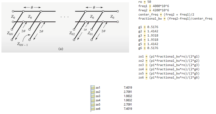
This formed the foundation for my ADS schematic.
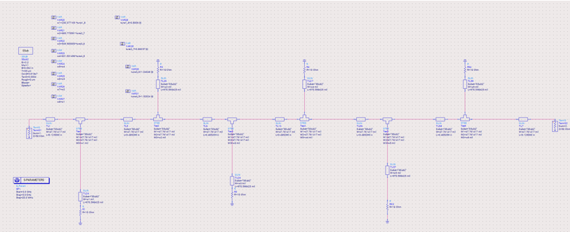
Step 2: Schematic-Level Simulation
In ADS, I built the schematic with stripline models (SLIN, SSUB, STEE, SSTEP). The half-wave OC stubs were open-ended striplines. Here’s where it got interesting: I adjusted the stub widths to shape the passband, tweaking their characteristic impedances to fine-tune the filter’s response. I added 1/8-inch 50-ohm lines at the input and output, then ran a 3–5 GHz sweep.
Here’s the schematic:
The results met the spec:
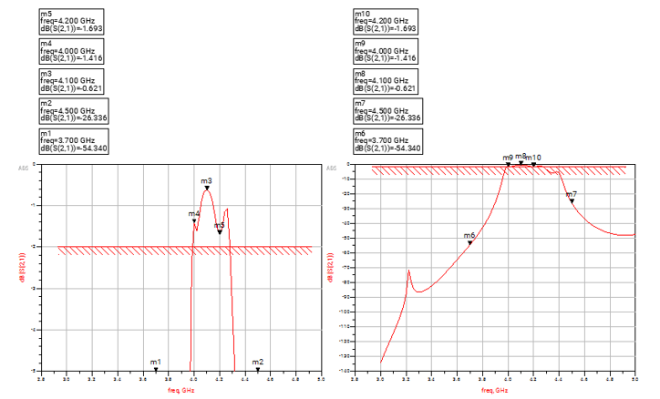
- Passband (4000–4200 MHz): S21 below 2.0 dB—check!
- Attenuation at 3.7 GHz: S21 beyond 35 dB—nailed it!
Tuning the stub widths was key to meeting all Table 1 specs—score!
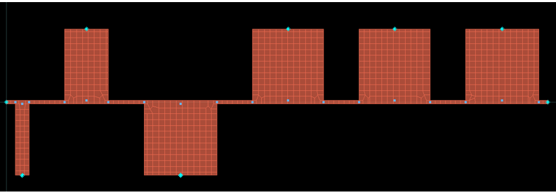
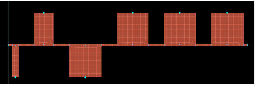
Step 3: Layout and EM Co-Simulation
I crafted the layout in ADS, translating the tuned stubs and coupled lines into stripline. Precision was critical—no gaps, no overlaps, and all features above 0.005 inches. Then, I ran the Momentum Microwave simulation over 3–5 GHz.
Here’s the layout:
And the EM results:
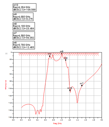
The EM run showed parasitic effects—stub width adjustments from the schematic didn’t translate perfectly due to coupling and substrate realities. Since EM didn’t need to hit the specs, this was a proof-of-concept win.
Takeaways
Adjusting stub widths to shape the passband was a game-changer—small tweaks, big impact. The EM phase highlighted how physical layouts challenge ideal designs. Ed Discussion with peers helped me nail down those width adjustments—collaboration for the win!